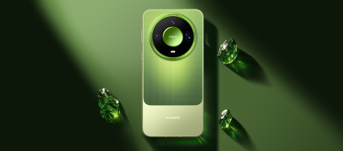
Did You Know
Did You Know: Huawei's Kirin 9050 Pro Is Really Two Chips Bonded Face to Face, With the Cache Folded Under the Cores
A lab cross-section of the chip inside the Mate 90 Pro Max found two same-size dies joined copper to copper, fed by about 80,000 vias. Huawei says the design cuts NPU power by as much as 66% at the same performance.
SHENZHEN, China · Kenji Watanabe, Did You Know · Oct 18 2026
SHENZHEN, China - Did you know the processor inside Huawei’s priciest new phones is not one slab of silicon but two, stacked face to face like the halves of a sandwich? When the Chinese review channel Geekerwan had a lab slice open the Kirin 9050 Pro from a Mate 90 Pro Max and rebuild its insides in 3D, it found a compute die and a second die of identical size bonded directly to each other, metal layer to metal layer, with copper-to-copper hybrid bonding. Huawei calls the approach LogicFolding and bills the Kirin 9050 Pro as the world’s first chip to use it.
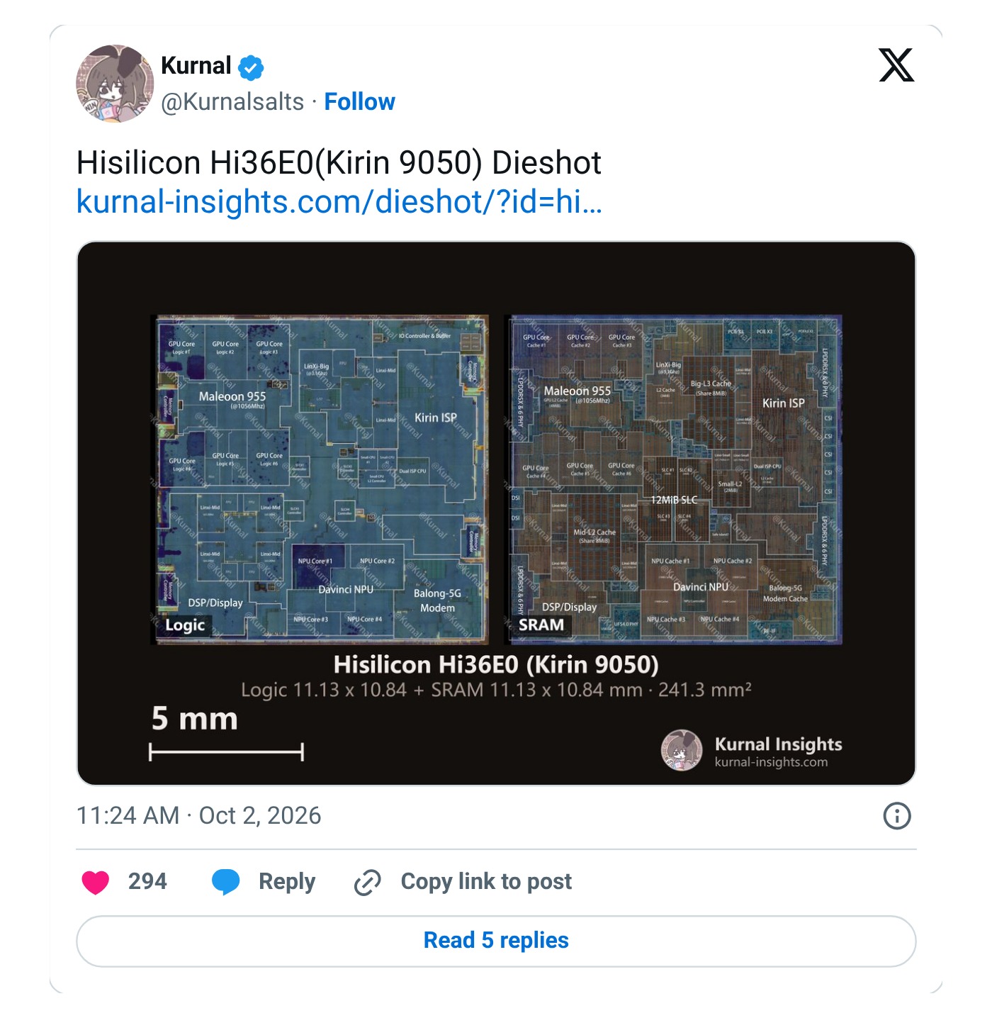 Screenshot: @Kurnalsalts on X
The surprise is how the work is divided. Stacking memory on a processor is not new; AMD’s 3D V-Cache puts a slab of extra cache on top of a finished CPU. Huawei folds each block in half instead. In the big CPU core, Geekerwan found the execution units on the top die and the core’s L1 and L2 caches on the bottom die, directly beneath the load/store units that feed them. Die shots posted on X by the semiconductor researcher Kurnal show the GPU and NPU split the same way. According to Tom’s Hardware’s reading of the teardown, the lower die also carries a shared L3, a 12MiB system cache, the clock circuits, and the interfaces for memory, cameras, display, storage and USB. Those parts run cooler and are less sensitive to the manufacturing process, so they go underneath. The hot compute sits on top, where heat escapes more easily.
 Image: Huawei
Getting power to a die that sits upside down between two layers of silicon takes a forest of wiring. Geekerwan counted about 80,000 through-silicon vias running through the lower die to reach the upper one, and says the vias and the keep-out zones around them use up about 8% of the bottom die’s usable area. Huawei’s own figure for the bonds between the two layers is far larger: its September announcement puts the vertical connections at about 50 million, at a hybrid-bonding pitch of 1.5 micrometers. Kurnal measured each die at 11.13 by 10.84 millimeters. That makes the chip’s footprint smaller than the previous Kirin’s, which Tom’s Hardware puts at more than 140 square millimeters, even though the two dies add up to about 241 square millimeters of silicon.
 Screenshot: @Huawei on X
Huawei says the shorter paths are the point. Its announcement says wire lengths fall about 20% on typical compute blocks and by up to 70% on some critical paths, and that at the same performance the chip uses 66% less power in the NPU, 58% less in the GPU and 41% less in a CPU performance core than its planar predecessor. Huawei also says transistor density rose from about 155 million to 238 million per square millimeter. Neither Huawei nor SMIC has confirmed the manufacturing nodes. Estimates cited by Notebookcheck and Wccftech put the compute die on SMIC’s N+3 process and the cache die on N+2, and Bloomberg, as cited by Tom’s Hardware, describes LogicFolding as a workaround for China’s lack of access to EUV lithography machines. Geekerwan measured the NPU at 68 TOPS of INT8 throughput.
*Video: Geekerwan on YouTube, the Kirin 9050 Pro cross-section and Mate 90 Pro Max tests (in Chinese)*Not everyone is sold on the branding. Ian Cutress, chief analyst at More Than Moore, wrote on X that Huawei’s “Tau scaling” idea is “a repackaging of what the industry has always done,” Tom’s Hardware reported. In a separate post, Cutress said a U.S. packaging company told him its standard tools already go beyond a 0.75-micrometer pitch. The chip has also drawn attention in Huawei’s new patent deal with Qualcomm: Bloomberg reported that some of the licensed Huawei patents underpin LogicFolding, while Qualcomm said on Oct. 6 that assertions linking the agreement to the technology are not accurate.
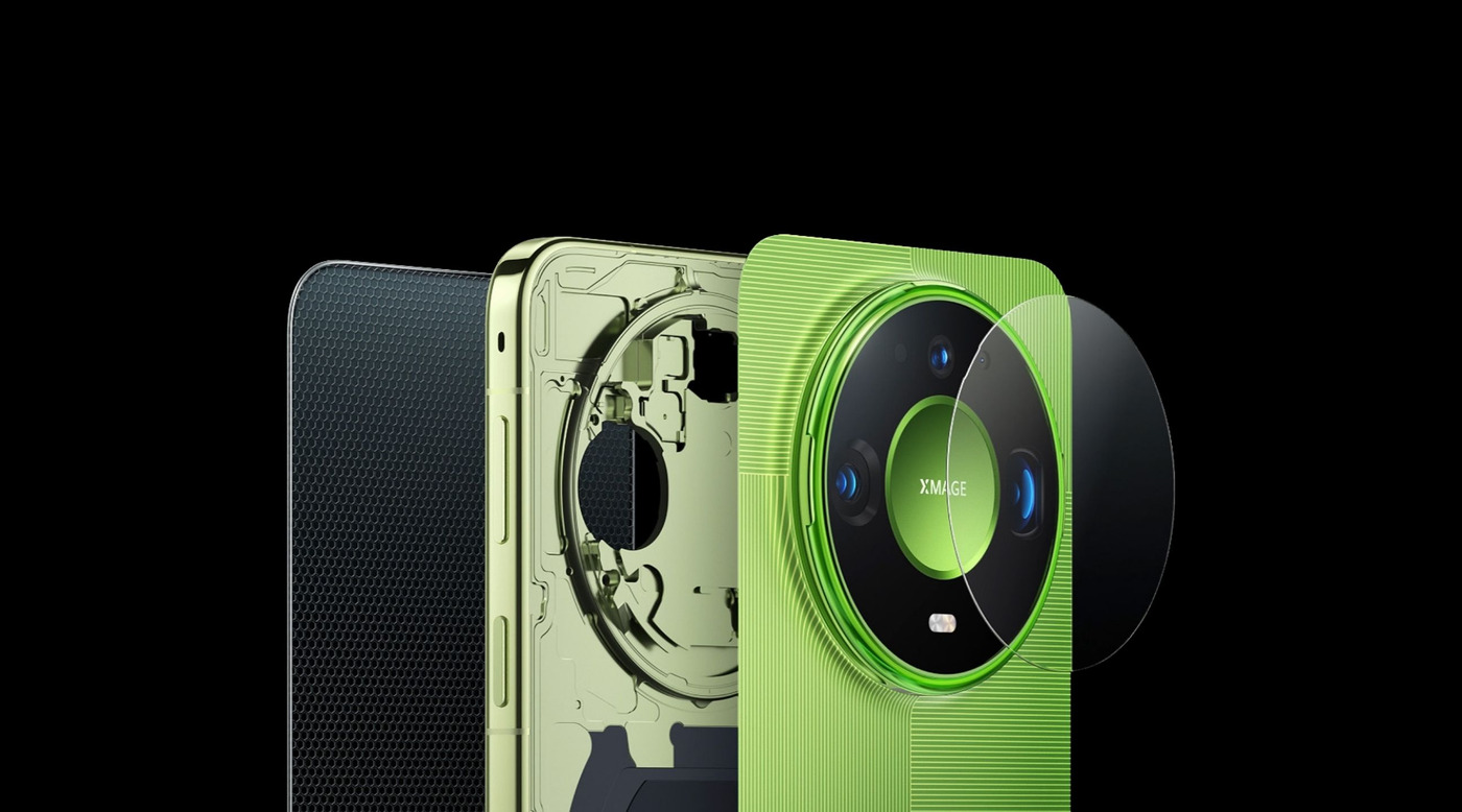
 Image: Huawei
Geekerwan cautioned that the technique is still expensive and that yields are still ramping, so for now it is reserved for flagship models; the Kirin 9030 and 9035 in the cheaper Mate 90 phones do not use it. Huawei says it already has silicon results for Kirin 2027, which shrinks the bonding pitch to 1 micrometer and lifts the vertical connections from about 50 million to more than 100 million. Its longer roadmap, according to Tom’s Hardware, targets 1.4nm-class transistor density by 2031. For a chipmaker locked out of the most advanced lithography tools, the next generation of phone performance is being built upward.
Sources: Huawei, “HUAWEI bringt LogicFolding-Chiparchitektur erstmals in die kommerzielle Anwendung” (in German), Sept. 9, 2026, https://www.huawei.com/de/news/2026/logicfolding-chiparchitektur-kommerzielle-anwendung; Huawei on X, Mate 90 series launch post, Oct. 5, 2026, https://x.com/Huawei/status/2107052717814567294; Geekerwan on YouTube, LogicFolding deep dive on the Mate 90 series chip (in Chinese), https://www.youtube.com/watch?v=PpNFmPcBYPY; Kurnal on X, “Hisilicon Hi36E0 (Kirin 9050) Dieshot,” Oct. 2, 2026, https://x.com/Kurnalsalts/status/2105967029861953597; Tom’s Hardware (Shane Downing), “Qualcomm will license patents behind Huawei’s LogicFolding chip architecture, report says,” Oct. 7, 2026, updated Oct. 12, https://www.tomshardware.com/tech-industry/semiconductors/qualcomm-will-license-patents-behind-huaweis-logicfolding-chip-architecture-report-says-the-kirin-9050-pro-already-uses-it-with-a-teardown-showing-its-lower-die-is-mostly-cache-and-i-o; Notebookcheck (Bui Giang), “Teardown shows Huawei Kirin 9050 Pro uses a 3D V-Cache-like stacked design for the SoC,” Oct. 3, 2026, https://www.notebookcheck.net/Teardown-shows-Huawei-Kirin-9050-Pro-uses-a-3D-V-Cache-like-stacked-design-for-the-SoC-and-the-results-are-impressive.1414228.0.html; Huawei Central (Emiko Matsui), “Huawei Kirin 9050 Pro teardown explains 3D stacked chip design in detail,” Oct. 5, 2026, https://www.huaweicentral.com/huawei-kirin-9050-pro-teardown/; Wccftech (Rohail Saleem), Kirin 9050 Pro die shots, Oct. 2, 2026, https://wccftech.com/die-shots-for-huaweis-latest-kirin-9050-pro-chip-show-a-much-smaller-footprint-encompassing-a-logic-die-on-smics-n3-process-bonded-to-an-sram-die-on-the-n2-process/; KOCPC, Geekerwan’s Kirin 9050 Pro logic-folding teardown, Oct. 3, 2026, https://en.kocpc.com.tw/archives/25948; Ian Cutress on X, Oct. 5, 2026, https://x.com/IanCutress/status/2107120690792935884.
Kenji Watanabe, Asia desk. Kenji Watanabe is a senior correspondent covering Asia tech, handsets, and platform software. Previously reported from Tokyo and Shenzhen for regional outlets; based in Tokyo.